My Journey within the Embedded Domain part 1
2017
Completing my Master’s degree in Embedded Systems
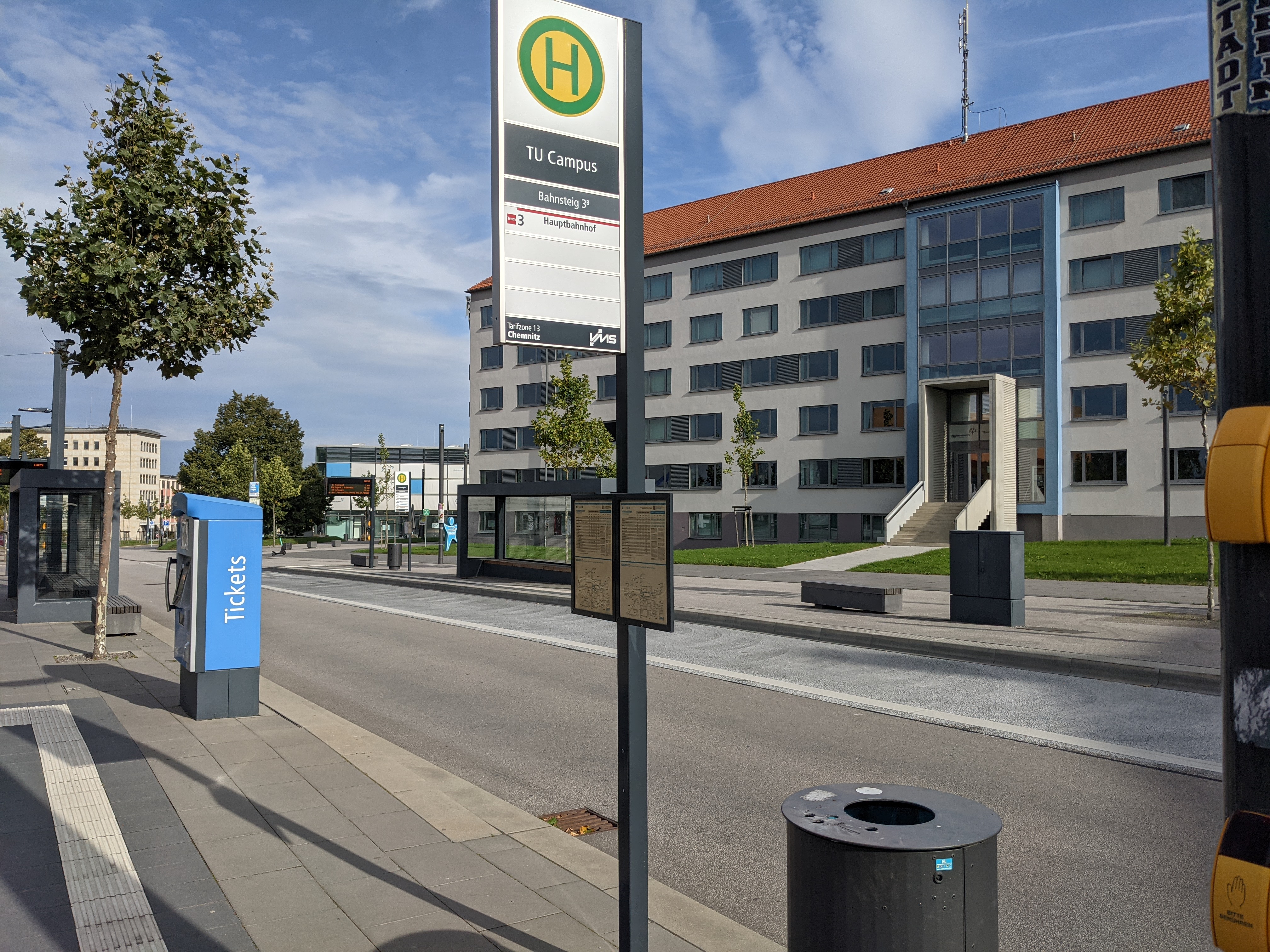
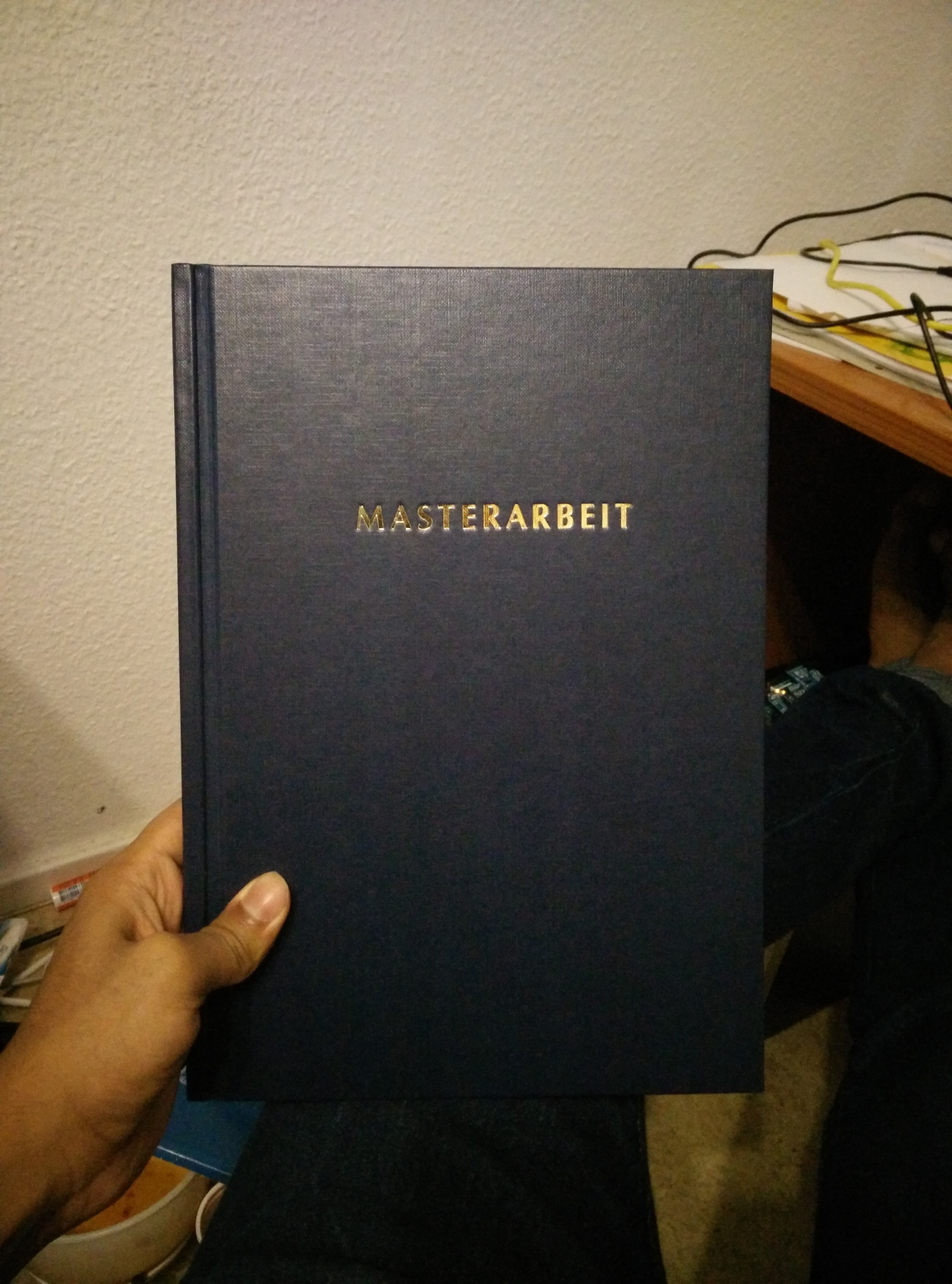
In 2017, I reached the final leg of my master’s degree in Embedded systems at TU Chemnitz, Germany. While working on my final research project and getting my master’s thesis ready for submission, I started applying for entry-level embedded software engineer positions within Germany.

Trying hard for a job
It won’t be a surprise to many reading this, in case you are unaware, the German Labor market for non-German speakers is incredibly unforgiving. After about 150+ applications to entry-level embedded software engineer roles and receiving not even one interview invitation, I focussed on the neighboring countries as well.
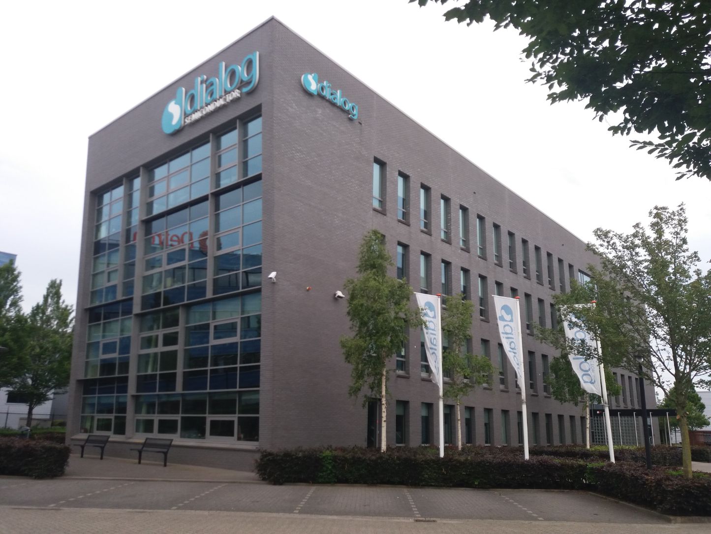
I applied for a graduate-level embedded software engineer role in The Dialog Semiconductors, located in Den Bosch, The Netherlands. I was pleasantly surprised when I was invited for a telephone interview. I spoke with my then-boss, Simon. We had a good chat together on both technical and non-technical items. Looking back, I regret my answer when he asked me where I saw myself in the next 5 years. I told him, “I would like to be where you are now, as a manager”. Sometimes, thinking back on this doesn’t even make me chuckle, rather embarrassed.
Simon invited me on-site for a technical interview. I met him and then teammates, Wik and Dennis. All three of them probed me with various basic embedded software and hardware-related questions. After the interview was complete, I went back to my student hostel in Chemnitz, Germany. In a month, I received word from the hiring team at Dialog Semiconductors that I was offered a role there. I happily accepted the role and moved on to formally complete my master’s degree as well.
My start in The Netherlands
In the last quarter of 2017, I moved to Den Bosch, The Netherlands to start my role as a graduate embedded software engineer. Simon, Dennis, and Wik welcomed me into their team. Simon, my direct boss is also responsible for at least 20+ engineers offshore. Our team directly reported to him.

Wik, the most senior talent on the team, originally started his career/profession as a mechanical engineer. Later down the line, by switching roles strategically he landed a role that mixed software and hardware. Dennis, almost 10 years older than me focused on electronics at the end of his academic journey, thus leading him to this team. Regarding our daily activities, Dennis focussed on developing bootloaders for a new range of microcontrollers that Dialog Semiconductors released to the market. Wik, on the other hand, took care of Direct Test Mode (Lower-level Bluetooth Low Energy stack) related tasks. Until quite recently before I joined, the company was famous for its wireless DECT-related solutions. They gradually saw potential with the low-powered BLE and switched to it.

first tasks on the job
During the start of my career and job, I was asked to start learning the local build and development ecosystem by familiarising myself with the DA14195 and DA14495 range of microcontrollers that had DECT radio capabilities and an Xtensa DSP processor inside along with an ARM cortex M0 for the CPU. Interestingly the units ran off a QSPI flash memory unit. This surprised me at the time as I hadn’t heard much about this specific QSPI controller yet. My teammates demonstrated the awesomeness of the peripheral when they probed a memory range associated with that peripheral and the unit responded with data in the memory range (from within the external QSPI flash) without any user intervention to handle the SPI flash commands. This type of boot-up mechanism and external peripheral handling impressed and amazed me. Meanwhile, along with a standard company-issued laptop, I was also provided with state-of-the-art debugging tools such as a logic analyzer, and Jlink debugger and access to a fully equipped scientific lab with even more serious/expensive test equipment.
Our sister team had an engineer Gerard, who has been in the industry for so long that he even used tapes to feed in and feed out computational tasks. Quite some years ago, maybe in the 90s, he was tasked with creating/developing a microcontroller evaluation suite that the engineers in the other departments could start and talk with their microcontrollers, probing their memory ranges, reading, and writing to specific memory ranges. The application was called DCTmon, and it was also capable of many things, notably the ability to take the in-house generated data sheet of the microcontrollers and display a visual tree of peripherals that the user can read and write to. I was tasked with learning, maintaining, and developing the in-house development tool as they didn’t have any active maintainers working on it.
As a maintainer of the internal characterization tool, I was also tasked with debugging/developing flash loaders for various old and new devices. I used the opportunity to develop a generic flash driver based on the JEDEC standard. Every FLASH memory device that was JEDEC compliant was able to operate with the generic flash loader.
The environment was conducive enough to encourage me to start a journey of learning embedded system (software and hardware) concepts and become experienced with them.
Before I conclude, What did Dialog Semiconductors do?
Dialog Semiconductors was previously Sitel Semiconductors which was previously National Semiconductors. From the time of Sitel and National, the firm has been specializing in bringing up low-power microcontrollers with power-efficient wireless technologies, mainly, DECT. Many home phones of yesteryear utilized these SOCs to be portable and easy to use throughout the home without being fixed to a wall. Soon after Dialog acquired the business unit in Den Bosch, they decided to explore the newly emerging market for Bluetooth Low Energy back in the 2014s. Dialog in other parts of the world had different products that it was manufacturing. Dialog’s PMIC ICs are quite famous. When I joined here in 2017, Dialog’s Den Bosch and Greece units were fully invested in the Bluetooth Low Energy market. They did not have any trouble attracting big names from China to procure their line of BLE-enabled MCUs.
The usual process is that, the engineering departments design and come up with IPs for their various flagship offerings. These IPs are packaged and sent to TSMC or GF somewhere in the world to be taped out. When the tape out is deemed successful, they are ready for mass manufacture orders. If the samples from the tape-out have problems during various testing runs, a metal layer change or something similar to a re-run has to be undertaken soon which costs lots of money, which is why people strive very hard to make it right the first time around.