My Journey within the Embedded Domain part 4
2020
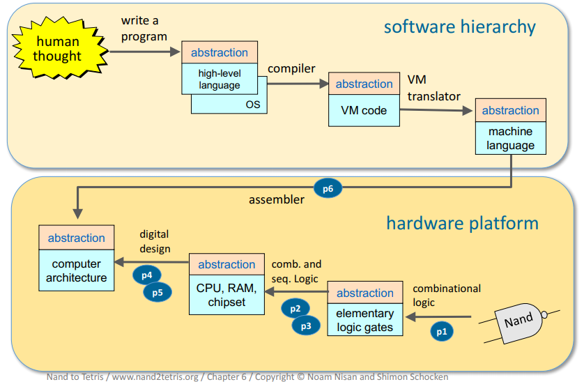
Nand2tetris
Having been in the professional embedded software development space for a little over 2 years, I started to experience a nagging sensation at the back of my mind that insisted I learn computer science engineering concepts from scratch once again. Looking back to that sensation, now, at this point in my life, I think it was mainly because I felt the imposter syndrome kicking in. I felt the much-experienced seniors around me knew what they were doing and that I didn’t. I don’t mean to say that I was not performing my assigned tasks to the best of my abilities, but rather a feeling of not fitting in with the much more intelligent/experienced seniors. Fortunately, I came across a course called Nand2Tetris, taught by professors Shimon Schocken and Noam Nisan on the Coursera platform, Nand2Tetris
This course was in essence, a completely self-contained course that starts theoretical explanations from NAND gates (implementing them in parallel using their verilog/VHDL style HDL language that is simulatable using a provided JAVA simulator program) to ALUs in the hardware level to bytecode execution on a custom virtual machine built during the course. As its name suggests, the course aims to build a Tetris game at the end, which would run on a computer designed while following the program. During the course, they introduce a low-level language called Hack and show how such a Hack Assembler could be created that can eventually construct machine code that runs on the Hack computer that this course helps design. In the second part of this course, the gears are shifted toward the software side of computer science engineering. The professors introduce the idea of a virtual machine and jack programming language. At the end of the course, you get fully satisfied knowing that you have participated in all the levels of computer science engineering to create a working model of a computer from scratch, literally.
This is a program that I often would like to revisit when I find more time to spare. I would highly advise the readers to try this out as well.
Diving more into Bluetooth Low Energy stack
At this point, I have had my fingers in multiple things: Bootrom testing assistance to Dennis, HTOL firmware development, ELFR firmware development, DCTMon C++ legacy maintenance, DCTMon python re-write, and some minor tasks here and there. Simon had decided that I was now ready to take on some big-boy tasks that Wik had been handling alone for several years.
I did introduce Wik to you, on my first page titled “My Journey within the Embedded Domain Part 1”. It does not do any justice to him. I have observed Wik closely for a while at this point and have seen him in action as well. He is the mere definition of a methodical engineer. Strangely, he did in fact like the art of debugging the firmware. If I took a problem that I encountered, to Wik, and when he had some time to look into it, his approach to debugging it looked so methodical and calculated. He is the very reason that I don’t sulk or feel doomed when the firmware I create/write doesn’t work as expected in the first run.
Wik worked on a lower-level layer of the BLE stack called Direct Test Mode. This is a layer of stack in the BLE that is meant to calibrate/verify/validate radio subsystems of the hardware on the production floor. The idea is that a user or in this case an expensive automated tester would send commands to the BLE DTM layer, through UART, USB, or any other communication protocol that the manufacturer implements. These commands will contain instructions to either transmit or receive custom BLE packets with custom RX/TX sensitivity, packet error rates, and a multitude of testing parameters.
Here is a quick representation of a common production line use-case of such protocol layer (extracted from Texas Instruments documents)
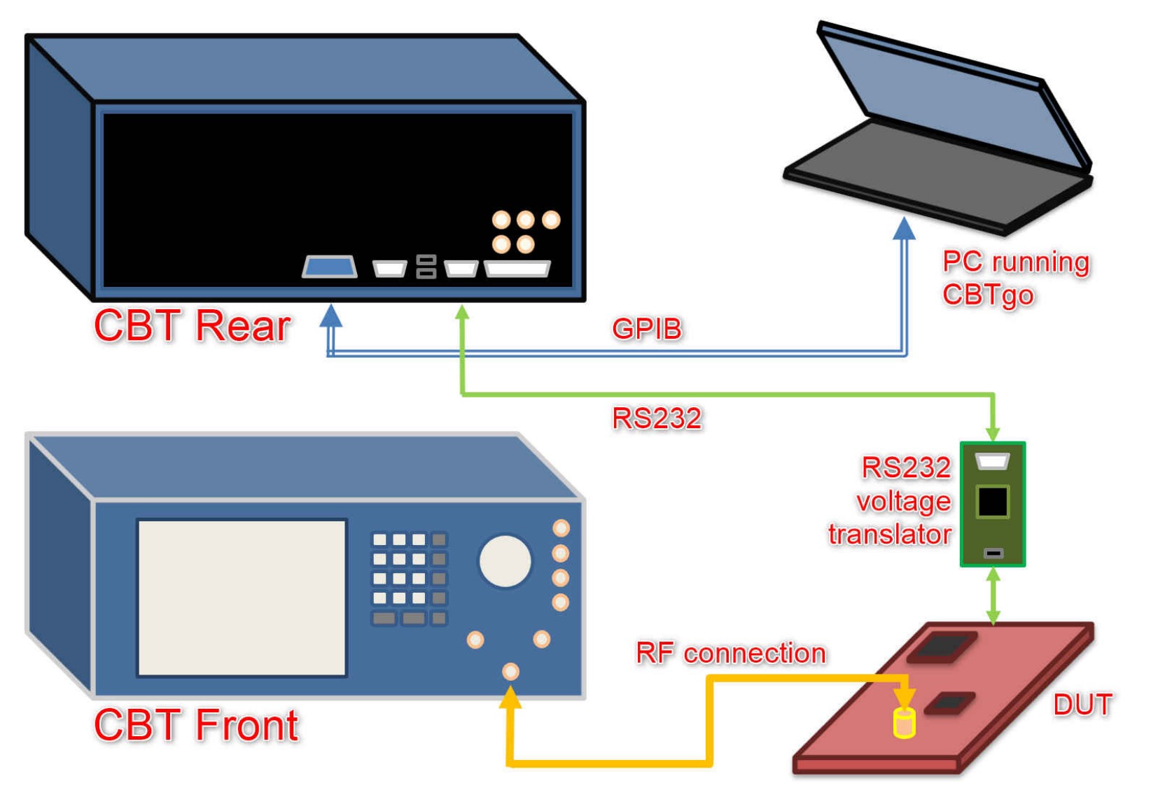
Various members of the radio design group frequently used the work that Wik created to verify/validate/test/characterize the radio system.
This is the instance where the rubber met the road. All the theories that I was introduced to about BLE through Robin Heydon’s book are observable now. At this point, I had a practical introduction to the various important concepts of BLE such as 625-microsecond timer slots for individual BLE packets, advertising channels, advertising intervals,server-client architecture, GATT, GAP, security, long-term/short-term bonding, key exchange, data channels, frequency hopping algorithms, GFSK modulation, 2.4GHz with 80MHz bandwidth in the ISM band, etc.,
PCB design
Halfway through the year, I was slowly hearing how great the Kicad PCB design program was shaping up. Everyone had good things to say about this. I wanted to try it out but I never really had a formal introduction to the subject. I stumbled upon a Udemy course from Dr.Peter Dalmaris called “KiCad Like a Pro 2nd edition”. I enjoyed the course from start to finish. The instructor covers the flow from the normal schematic stage to the PCB layout and routing stage.
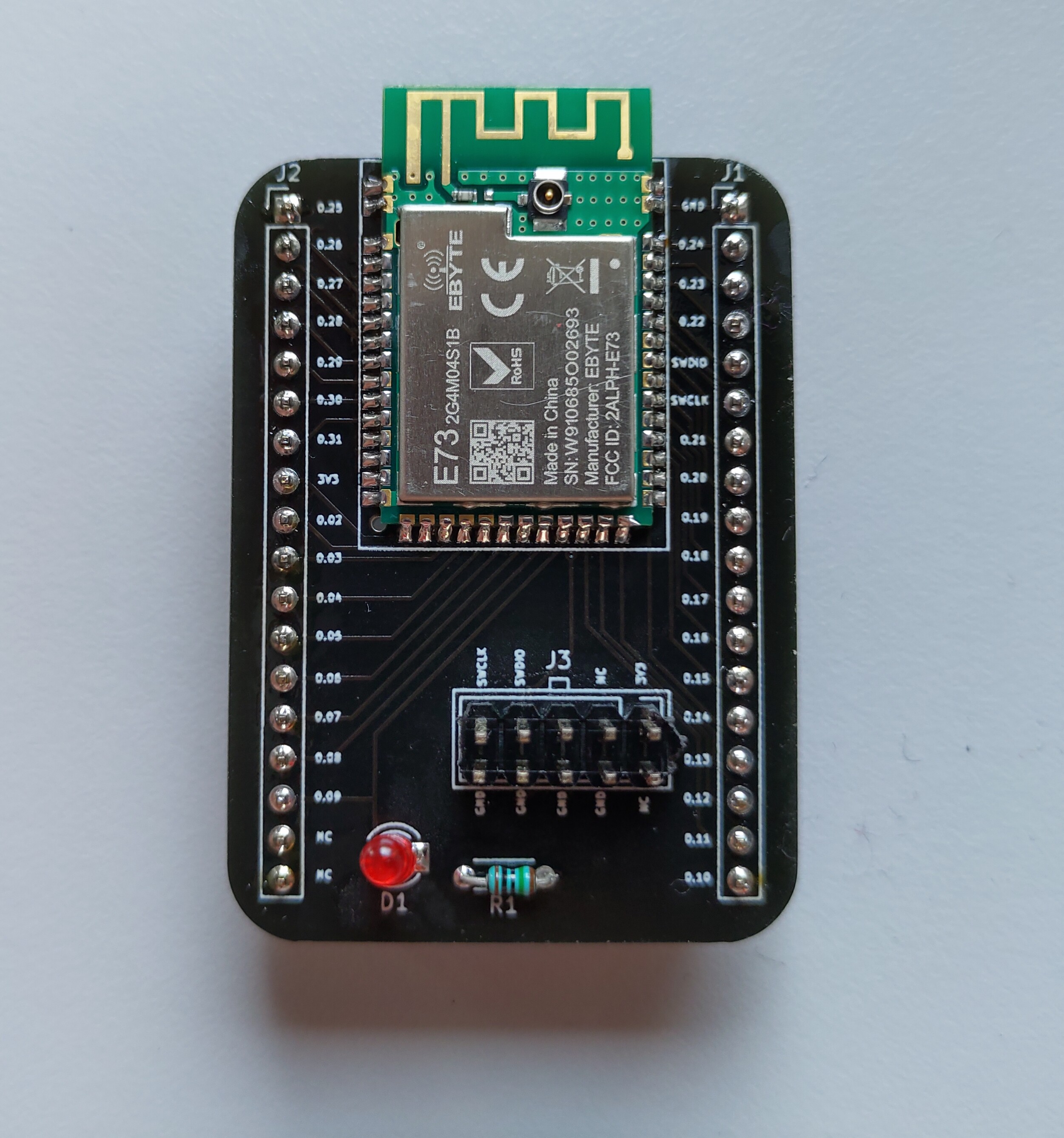
As I had started this year to experiment heavily with BLE, I wanted to do something on the same line with the PCB design experimentation. I found a Nordic BLE module in Aliexpress. I decided to create a base board for this module to use my newfound PCB design. I created a base board and sent it to JLCPCB in China. The first run had a quick problem with the SWD connectors. The connectors had a smaller footprint than the intended one.
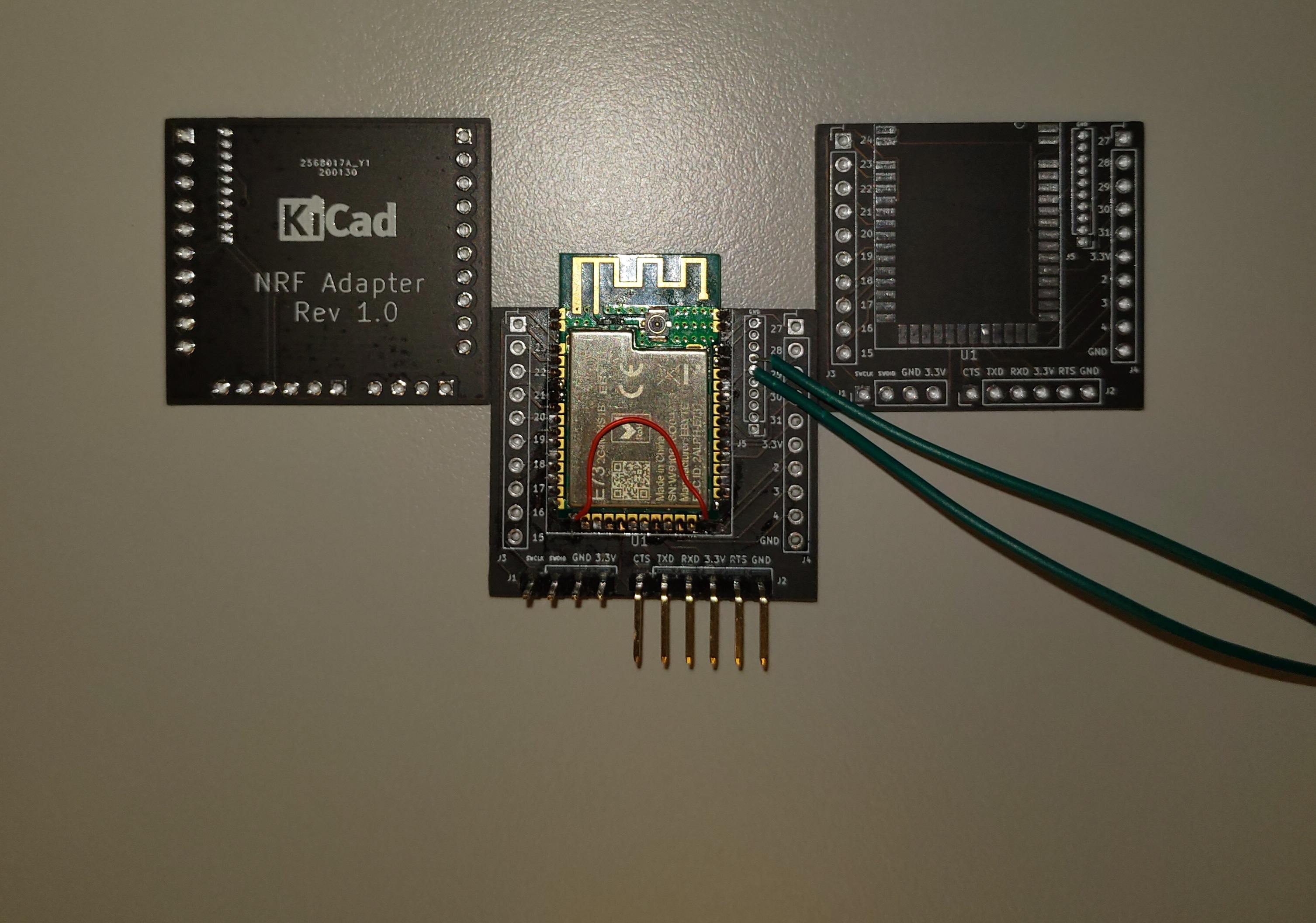
I quickly re-did and corrected the design and had it manufactured. This time, everything went ok and my first PCB design was indeed successful.
Dr. Peter also displays my PCB on his webpage over here: NRF52 Base board
Secure boot
When a more powerful successor for the flagship DA1469X was planned, Dennis was tasked with the bootrom creation once again. This time around, the bootrom should handle secure boot features as well. Here are some videos from YouTube to help you get the basics of secure boot:
Here are some un-edited notes that I created for myself during this learning experience:
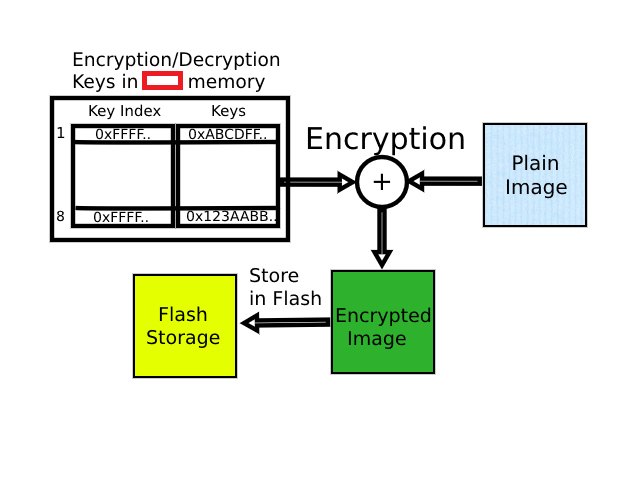
Assume that the user has their bootable image ready. To prevent this firmware image from being counterfeited, the image is first cryptographically secured. This type of cryptographic encryption is symmetric as the same key used for the encryption is used for decryption. This new chip will have dedicated secret storage for the encryption/decryption keys. The encryption/decryption key index table in combination with the encryption/decryption key area holds enough space for 8 (4 bytes) index values and 8 (64 bytes) keys. Using one of the encryption/decryption keys that were stored inside the secure area of the chip, the user encrypts the bootable image and stores it in the QSPI/OQSPI Flash device.
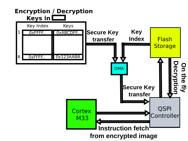
Ideally, we configure the on-the-fly-decryption feature that uses a dedicated DMA channel to retrieve the key and decrypt the image on the fly.
Some more notes on signature generation and validation:
To render the device tamper-proof, certain signature creation and validation procedures are performed.
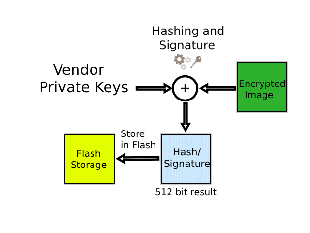
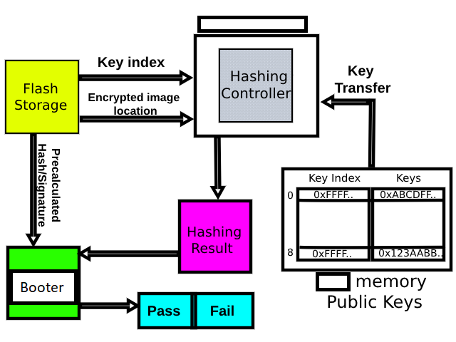
Every public key that resides in the secret storage area has a unique private key. A public key can be derived from the private key, but the private key cannot be derived back from a public key. Hence, they are mostly referred to in pairs. Using the public/private key pair and an encrypted/plain image the user creates a signature by using the appropriate hashing/signature algorithm. The resulting 256/512-bit signature is then stored along the bootable image inside the flash storage. During the boot procedure, the booter checks if the product/image header holds security data. If it does, First, the booter tries to validate/verify the signature of the bootable image present in the flash device.
The booter takes care of signature validation/verification. The booter is configured to use hardware AES hashing peripheral along with the basic location details of the bootable image start address and the stored signature that is used to compare the result of the signature verification/validation procedure. The public keys are also safely transferred to the hashing controller during the process.
Finally, the booter compares its result on the hashing/signature generation of the encrypted image with the already stored signature. If they are the same, the bootable image has not been tampered with. If the results are different then the image has been tampered with.
After everything was said and done, I still was able to freshen up my knowledge on the cortex-M family through an Udemy course from Kiran titled “Master Microcontroller with Embedded Driver Development”.